Showing posts with label Si570. Show all posts
Showing posts with label Si570. Show all posts
Saturday, October 1, 2016
Updated Si570 code on GitHub
Well, I have finally updated my Si570 code on GitHub to reflect the changes to fix a bug found and blogged about over two years ago. I described the fix here, but failed to follow through and update the code on GitHub with the changes. Long past due, but glad to have that task off my TODO list.
Sunday, December 28, 2014
BPSK vs. FSK/MSK
In a previous post I pondered briefly about BPSK (used in PSK31) as compared to FSK. Instead of traditional frequency-shift keying, in BPSK information is transmitted by patterns of polarity-reversals (sometimes called 180-degree phase shifts). One way to think about this would be to swap antenna terminals on each phase reversal.
BPSK uses a 180 degree phase shift when encoding a zero bit in a varicode character. By way of review, BPSK uses a sinusoid of constant amplitude and a 180 degree phase shift to represent a binary 1 as opposed to a binary 0.

Now, the problem with this in radio circuits is the phase reversal if hard keyed will result in a lot of splatter and the accompanying bandwidth. So, in radio circuits as discussed in my series about PSK31 on the arduino, we typically ramp the sinusoid level down to zero at the phase change points to eliminate this splatter and shift the phase reversal to the middle of the bit time. PSK31 encodes a zero bit as a phase reversal and a one bit as no phase change. In other aspects however PSK31 is BPSK.

In thinking about BPSK vs. FSK or more accurately, MSK (Minimum Shift Keying) I found myself pondering whether they are functionally equivalent.
MSK is basically FSK with the shift set to ½ the baud rate. Realistically this is the smallest shift you can use without trading off transmission speed. PSK31 uses a 31.25 baud transmission speed. So, if we were going to encode a 31.25 baud data transmission using MSK, our keying shift would be 1/4 of the data rate either side of the transmit center frequency.
31.25 baud / 2 = 15.625 / 2 = 7.8125 Hz
If you think of the phase of a carrier that is 7.8125 Hz below the transmit center frequency, it will lag by 90 degrees after 32 mS, and at 7.8125 Hz above, it will lead by 90 degrees after 32 mS for a difference of 180 degrees.
So MSK appears to be functionally equivalent to BPSK while using +90 and -90 degree shifts instead of 0 and 180 degree shifts.
An advantage to this approach is that the resultant signal has no amplitude modulated component and so non-linear amplification techniques may be utilized greatly simplifying transmitter design. It does require the ability to do phase continuous frequency changes however.
Hmm...
Ok, so to give this concept a play around, I decided to use all the recent work I did on the Minima to implement 1 Hz tuning on the Si570 and see if I could implement a decode-able PSK31 varicode message using MSK techniques with the Si570.
The Si570 is technically capable of 0.42 Hz frequency precision, but for this experiment, I will use 8 Hz as the frequency shift above and below the transmit frequency instead of 7.8125 Hz.
At 7.8125 Hz, 360 degrees of phase change takes 128 ms. 90 degrees of phase change requires 128/4 = 32 ms.
At 8 Hz, 360 degrees of phase change takes 125 ms. 90 degrees of phase change requires 125/4 = 31.25 ms.
I suspect that most PSK31 decoding applications will be able to deal with this difference.
Having modified my recent PSK31 code to drive the Si570 oscillator rather than generate audio, I have run into a number of problems. I suspected that the i2c communications library that comes with the Arduino IDE would require interrupts to be enabled, which is true. If you try to call the Si570 code from within a timer interrupt, it will hang the device.
Enabling interrupts around the Si570 call within the timer ISR cures the hanging problem, but fails to communicate with the Si570 to set the frequency. I suspect that while the library is returning quickly, the i2c communications doesn't complete until sometime later.
Moving the setFrequency() call out of the ISR generates MSK, but it appears that there are bits being lost. The ISR is completing in 1.040 us, but is not accurately generating all of the frequency shifts. My suspicion is that the wire library is returning quickly, but that its own interrupt are not completing in a timely fashion to allow precise control over when frequency shifts are happening. I will have to do some measurements on the i2c communications and put some debugging pin toggles in the wire library to measure how long things are taking to complete.
More to come...
BPSK uses a 180 degree phase shift when encoding a zero bit in a varicode character. By way of review, BPSK uses a sinusoid of constant amplitude and a 180 degree phase shift to represent a binary 1 as opposed to a binary 0.
Now, the problem with this in radio circuits is the phase reversal if hard keyed will result in a lot of splatter and the accompanying bandwidth. So, in radio circuits as discussed in my series about PSK31 on the arduino, we typically ramp the sinusoid level down to zero at the phase change points to eliminate this splatter and shift the phase reversal to the middle of the bit time. PSK31 encodes a zero bit as a phase reversal and a one bit as no phase change. In other aspects however PSK31 is BPSK.
In thinking about BPSK vs. FSK or more accurately, MSK (Minimum Shift Keying) I found myself pondering whether they are functionally equivalent.
MSK is basically FSK with the shift set to ½ the baud rate. Realistically this is the smallest shift you can use without trading off transmission speed. PSK31 uses a 31.25 baud transmission speed. So, if we were going to encode a 31.25 baud data transmission using MSK, our keying shift would be 1/4 of the data rate either side of the transmit center frequency.
31.25 baud / 2 = 15.625 / 2 = 7.8125 Hz
If you think of the phase of a carrier that is 7.8125 Hz below the transmit center frequency, it will lag by 90 degrees after 32 mS, and at 7.8125 Hz above, it will lead by 90 degrees after 32 mS for a difference of 180 degrees.
So MSK appears to be functionally equivalent to BPSK while using +90 and -90 degree shifts instead of 0 and 180 degree shifts.
An advantage to this approach is that the resultant signal has no amplitude modulated component and so non-linear amplification techniques may be utilized greatly simplifying transmitter design. It does require the ability to do phase continuous frequency changes however.
Hmm...
Ok, so to give this concept a play around, I decided to use all the recent work I did on the Minima to implement 1 Hz tuning on the Si570 and see if I could implement a decode-able PSK31 varicode message using MSK techniques with the Si570.
The Si570 is technically capable of 0.42 Hz frequency precision, but for this experiment, I will use 8 Hz as the frequency shift above and below the transmit frequency instead of 7.8125 Hz.
At 7.8125 Hz, 360 degrees of phase change takes 128 ms. 90 degrees of phase change requires 128/4 = 32 ms.
At 8 Hz, 360 degrees of phase change takes 125 ms. 90 degrees of phase change requires 125/4 = 31.25 ms.
I suspect that most PSK31 decoding applications will be able to deal with this difference.
Having modified my recent PSK31 code to drive the Si570 oscillator rather than generate audio, I have run into a number of problems. I suspected that the i2c communications library that comes with the Arduino IDE would require interrupts to be enabled, which is true. If you try to call the Si570 code from within a timer interrupt, it will hang the device.
Enabling interrupts around the Si570 call within the timer ISR cures the hanging problem, but fails to communicate with the Si570 to set the frequency. I suspect that while the library is returning quickly, the i2c communications doesn't complete until sometime later.
Moving the setFrequency() call out of the ISR generates MSK, but it appears that there are bits being lost. The ISR is completing in 1.040 us, but is not accurately generating all of the frequency shifts. My suspicion is that the wire library is returning quickly, but that its own interrupt are not completing in a timely fashion to allow precise control over when frequency shifts are happening. I will have to do some measurements on the i2c communications and put some debugging pin toggles in the wire library to measure how long things are taking to complete.
More to come...
Thursday, October 23, 2014
Minima controller shield - Using second Si570 as BFO.
I have implemented changes to the Minima controller code developed by Eldon Brown (WA0UWH) and others to use the second Si570 on my controller shield as the BFO oscillator. This change allows easy setting of your Minima BFO oscillator frequency to the desired point on your crystal filter passband curve, be that at the -3 dB point or further down the skirt.

The IF edit mode of the controller firmware will allow the adjustment of the BFO frequency. Separate frequencies are maintained for USB and LSB.
A separate issue is regarding the calibration of both of the Si570 devices on the shield against some frequency standard. For most folks that have a crystal oscillator for the BFO, the IF edit mode has probably been used to calibrate the dial to some frequency standard and this is fine. However adjusting the IF frequency offset from the displayed frequency only allows you to match the value that the controller uses to whatever frequency your crystal oscillator BFO is tuned to whereas with the second Si570, you can actually move the BFO frequency in software which is not the same thing as calibrating the dial.

The calibration of the Si570 devices as I see it is a separate matter from setting the desired BFO frequency as you certainly don't want to change where the BFO frequency sits on the IF passband just to calibrate the dial. So, I anticipate providing a different mechanism that will allow moving the VFO frequency (and BFO frequency for those using a second Si570 as the BFO oscillator) without changing the displayed frequency in order to determine the error offset for each Si570. This error offset can then be stored in eePROM and applied automatically from that point forward to the appropriate Si570.
More to come on this topic...
Saturday, September 20, 2014
Minima Controller Shield - mounting options
Well, I am not certain yet how I am going to mount things in the long run, but for now I have stacked the display, Uno and Shield on the back of the panel. My wires are deliberately long until I make a final decision, but for now I have just coiled them up.


I will most likely fashion another panel a little bit larger that will have room for more buttons as well as the rotary encoder at which time the current tuning pot will become the speed control for a keyer. I have located some scrap aluminum, so I think it is the next best step.
Friday, September 19, 2014
Minima working with new shield
This evening, I hacked poor Wayne, NB6M's Minima to accept VFO energy from my Minima Controller shield. As a first hack, it worked fine and I was able to test drive the receiver from my controller.

I disconnected Wayne's Si570 output and brought the coax out to an SMA connector that I hooked up with a short SMA jumper cable to my VFO output. Other than being out of calibration, it seems to work fine.

So far so good... I want to try using the second Si570 as the BFO, but more surgery is necessary in order to replace the BFO oscillator. I think I will wait until I am more awake...
I disconnected Wayne's Si570 output and brought the coax out to an SMA connector that I hooked up with a short SMA jumper cable to my VFO output. Other than being out of calibration, it seems to work fine.
So far so good... I want to try using the second Si570 as the BFO, but more surgery is necessary in order to replace the BFO oscillator. I think I will wait until I am more awake...
Monday, September 8, 2014
Minima Controller Shield - Some measurements
Last evening I placed my second Si570 on my Minima Controller shield and am pleased to see it is functional as well.


The datasheet for the Si570 CMOS version says that supply current draw should typically be 90 mA with a maximum of 98 mA. With both devices powered up, I am seeing a current draw on the 3V3 rail of 140 mA.
The Arduino UNO R3 board uses a TI LP2985-33DBVR regulator which according to its datasheet is rated for 150 mA. There is nothing on the Arduino board that uses 3V3, but given the maximum current draw of two Si570 devices at 196 mA drove the decision to install a separate 3V3 800 mA regulator on the board. At my current draw, I might be able to get away with using the Arduino 3V3 rail, but it is pushing things. Another option might be to replace the regulator but again, I didn't want to modify the Arduino board.
Interestingly, the Arduino documentation says not to draw more than 50 mA from the 3V3 rail which makes me suspect that they may have trimmed the heat sink tab on the part.
Interestingly, the Arduino documentation says not to draw more than 50 mA from the 3V3 rail which makes me suspect that they may have trimmed the heat sink tab on the part.
I am seeing 13.5 dBm with no attenuation out of the Si570 devices so there is plenty of drive available to allow experimentation with different mixers. The PI pad resistors can be populated to set any level desired.
I have Wayne, NB6M's Minima build at my disposal for a few weeks to be able to try out the new shield for both VFO and BFO signal sources and am looking forward to seeing how this works out in a practical sense.
Sunday, September 7, 2014
Minima Controller Shield checkout
UPDATED:
My Minima controller Arduino shield checks out as functional. With two Si570 devices on the board, powering them from the Arduino regulator is pushing things, so I have isolated the 3V3 rail from the Arduino and provided my own regulator. However, with only a single Si570 on the board, I am within limits on the Arduino regulator. Therefore, I jumpered the power input pin back to the Vin pin on the Arduino to supply power to the shield. This is the brown jumper wire seen below. The yellow wire is the ground to my scope probe.

Measuring the voltage off the regulator and the Si570 look good. Probing the output of the Si570 as seen above, we have the following default frequency of 56.32 MHz output seen below.

For those following along, the schematic of the shield looks like this. There really isn't anything to it. Just a multiplexer in front of two Si570's, voltage regulation and breaking out some of the I/O pins to separate cable connections for the Minima.

Now to go figure out how to talk to the multiplexer and the Si570.
I removed the shield from the Arduino Uno and connected up a bus pirate to see if I can talk to the PCA9546. When searching the I2C address space for devices, initially I got a "response" from all possible addresses. Clearly this is wrong...
Probing the PCA9546 I found that the voltages were correct, but that the reset pin was held low. As seen from the schematic above, this is connected to the reset button and the ICSP reset pin. However, this pin on the shield is not pulled up to any voltage rail and currently relies on the connected UNO to supply this voltage. So, rather than power the shield from the bus pirate, I plugged it back into the UNO and reinstalled my brown power jumper and just monitored SCL and SDA pins with the bus pirate.

Now interrogating the bus yielded the following results:
Bus Pirate v3
Firmware v4.2 Bootloader v4.2
DEVID:0x0447 REVID:0x3043 (B5)
http://dangerousprototypes.com
I2C>(1)
Searching 7bit I2C address space.
Found devices at:
0xE0(0x70 W) 0xE1(0x70 R) 0xFE(0x7F W) 0xFF(0x7F R)

My Minima controller Arduino shield checks out as functional. With two Si570 devices on the board, powering them from the Arduino regulator is pushing things, so I have isolated the 3V3 rail from the Arduino and provided my own regulator. However, with only a single Si570 on the board, I am within limits on the Arduino regulator. Therefore, I jumpered the power input pin back to the Vin pin on the Arduino to supply power to the shield. This is the brown jumper wire seen below. The yellow wire is the ground to my scope probe.
Measuring the voltage off the regulator and the Si570 look good. Probing the output of the Si570 as seen above, we have the following default frequency of 56.32 MHz output seen below.
For those following along, the schematic of the shield looks like this. There really isn't anything to it. Just a multiplexer in front of two Si570's, voltage regulation and breaking out some of the I/O pins to separate cable connections for the Minima.
Now to go figure out how to talk to the multiplexer and the Si570.
I removed the shield from the Arduino Uno and connected up a bus pirate to see if I can talk to the PCA9546. When searching the I2C address space for devices, initially I got a "response" from all possible addresses. Clearly this is wrong...
Probing the PCA9546 I found that the voltages were correct, but that the reset pin was held low. As seen from the schematic above, this is connected to the reset button and the ICSP reset pin. However, this pin on the shield is not pulled up to any voltage rail and currently relies on the connected UNO to supply this voltage. So, rather than power the shield from the bus pirate, I plugged it back into the UNO and reinstalled my brown power jumper and just monitored SCL and SDA pins with the bus pirate.
Now interrogating the bus yielded the following results:
Bus Pirate v3
Firmware v4.2 Bootloader v4.2
DEVID:0x0447 REVID:0x3043 (B5)
http://dangerousprototypes.com
I2C>(1)
Searching 7bit I2C address space.
Found devices at:
0xE0(0x70 W) 0xE1(0x70 R) 0xFE(0x7F W) 0xFF(0x7F R)
Checking the PCA9546 datasheet, we see the following:
If you look at the schematic above, you will notice that I connect A0-A2 to ground, so the device address should be 0x70 (this value is the 0xE0 shifted right one bit to remove the read/write bit) and the read/write addresses should be 0xE0 for write and 0xE1 for read.
So, it looks like the PCA9546 can be seen on the bus and so now it might be time to write some actual code.
Saturday, September 6, 2014
Minima Controller Shield Build
I have completed (as far as I went) the build of my Minima Controller Shield, but have yet to complete testing of the board. I populated only a single Si570, the edge and ICSP stackable headers and the header for my OLED display.

The prototype board needs a little work. I need to move the VFO SMA edge connector away from the USB connector. This will work for a prototype, but needs to move in the final version for sure.

The OLED display is a 3V3 device and I have it sharing the same I2C bus as the first Si570 for the VFO. There is also a 5V set of connections for an LCD display with an I2C backpack for example. This shares the same I2C bus as the PCA9546 multiplexer input, so it should allow 5V displays to work without driver modifications. I will need to customize the 3V3 OLED driver to take into account that it is connected to the PCA9546 multiplexer. I used this device because it allows voltage level conversion with a 5V input side and four 1.8 - 5V or more output side I2C buses. It also allows me to address multiple devices that do not allow you to change their I2C address such as the Si570. Without it, one would be limited to a single Si570 on a bus.

Ok, off to do some voltage testing and then to see if I can address the PCA9546. If so, I will get busy on my display driver changes and testing the Si570. I plan to roll my changes back into my Si570 driver to allow multiple instances behind a multiplexer as a compile time option.
The prototype board needs a little work. I need to move the VFO SMA edge connector away from the USB connector. This will work for a prototype, but needs to move in the final version for sure.
The OLED display is a 3V3 device and I have it sharing the same I2C bus as the first Si570 for the VFO. There is also a 5V set of connections for an LCD display with an I2C backpack for example. This shares the same I2C bus as the PCA9546 multiplexer input, so it should allow 5V displays to work without driver modifications. I will need to customize the 3V3 OLED driver to take into account that it is connected to the PCA9546 multiplexer. I used this device because it allows voltage level conversion with a 5V input side and four 1.8 - 5V or more output side I2C buses. It also allows me to address multiple devices that do not allow you to change their I2C address such as the Si570. Without it, one would be limited to a single Si570 on a bus.
Ok, off to do some voltage testing and then to see if I can address the PCA9546. If so, I will get busy on my display driver changes and testing the Si570. I plan to roll my changes back into my Si570 driver to allow multiple instances behind a multiplexer as a compile time option.
Thursday, September 4, 2014
Small Progress on the Minimal Controller Shield
I had a little time this evening to start stuffing my prototype Minima controller board with parts. Got the Si570, voltage regulator, reset button and PCA9546 I2C multiplexer installed. The rest is connectors and a few R and C 0805 parts. Getting there...

Progress on laying out my RF board for the Minima has been stalled for a couple weeks. I hope to get back on that before too much more time has passed.
Progress on laying out my RF board for the Minima has been stalled for a couple weeks. I hope to get back on that before too much more time has passed.
Monday, August 11, 2014
Si570 Arduino Shield PCB is off to be manufactured
I finished up the Si570 shield for the Arduino today and sent the gerber files off the the fab house today. They will be on the panel to be produced on 13 Aug, so hopefully I will have some prototype PCBs back soon.

Update: My prototype boards shipped yesterday (Friday) so hopefully they will be in hand by Monday.
Update: My prototype boards shipped yesterday (Friday) so hopefully they will be in hand by Monday.
Sunday, August 10, 2014
Si570 shield progress
I have spent some time today working on my Si570 Arduino shield. A few changes:
I however also included individual connections for individual periphery (encoder, paddles, buttons, PTT, etc.) so that a cable with a ground and signal lines can be connected as a single connector without having to worry about multiplexing ground lines, etc.
Using the I2C multiplexor will require a change to my Si570 driver and OLED driver. 5V I2C displays will not require any code changes as they will be connected directly to the 5V Arduino I2C bus.
Here is a quick screen shot of the board. It is pretty close to being ready to send off the be manufactured.

I am hoping to get these off to be created this week.
- Added a 3.3V regulator on the board with a separate power input (9-12v) as with dual Si570 devices on the board, I don't want to draw that current from the Arduino regulator.
- Increased the trace size for the 3V3 power rail off the regulator.
- Changed the SMA connector footprint to be appropriate for a much more narrow connector.
- I2C multiplexor chip used to drive multiple (up to 4) I2C buses optionally at different logic levels. I drive the multiplexor at 5V from the Arduino. Each Si570 is on its own 3V3 bus and two extra busses are available. I included the 3V3 OLED display on the first Si570 bus.
- Hand routing of the mess made by the Eagle auto-router.
- Replace reset button with one that is actually available.
- Rework the SMA connector footprint a little more as it is still marginally too wide.
I however also included individual connections for individual periphery (encoder, paddles, buttons, PTT, etc.) so that a cable with a ground and signal lines can be connected as a single connector without having to worry about multiplexing ground lines, etc.
Using the I2C multiplexor will require a change to my Si570 driver and OLED driver. 5V I2C displays will not require any code changes as they will be connected directly to the 5V Arduino I2C bus.
Here is a quick screen shot of the board. It is pretty close to being ready to send off the be manufactured.
I am hoping to get these off to be created this week.
Monday, August 4, 2014
Bug found in Si570 code for Minima
A problem has been discovered in my Si570 code that implements 1Hz tuning. The code was unnecessarily resetting the DCO on every update when tuning down in frequency. While setting the frequency correctly, the error was causing the DCO to restart on every increment in frequency producing an audible click in the Minima. The frequency was being set correctly, just clicking the receiver when it was not necessary.
The error was two-fold. Firstly, I failed to reserve sufficient bits for the 3500 ppm calculation. Secondarily, the Arduino absolute value function (abs()) is very quirky and it was just simpler to remove the function from my code.
Lastly, I modified the Si570 code to only calculate the 3500 ppm offset whenever the DCO centre frequency was changed rather than on every frequency change in order to gain a slight performance improvement.
The changes will be posted to my GitHub Si570 repository as soon as I am able. Meanwhile, here are the changes for the adventurous among us that want to take on the change manually.
In Si570.h, I added a member variable to the Si570 class to hold the calculated 3500 ppm value for the current center frequency.
class Si570
{
public:
Si570(uint8_t i2c_address, uint32_t calibration_frequency);
Si570_Status setFrequency(uint32_t newfreq);
void debugSi570();
Si570_Status status;
private:
uint8_t i2c_address;
uint8_t dco_reg[13];
uint32_t f_center;
uint32_t frequency;
uint16_t hs, n1;
uint32_t freq_xtal;
uint64_t fdco;
uint64_t rfreq;
uint32_t max_delta;
uint8_t i2c_read(uint8_t reg_address);
int i2c_read(uint8_t reg_address, uint8_t *output, uint8_t length);
void i2c_write(uint8_t reg_address, uint8_t data);
int i2c_write(uint8_t reg_address, uint8_t *data, uint8_t length);
bool read_si570();
void write_si570();
void qwrite_si570();
uint8_t getHSDIV();
uint8_t getN1();
uint64_t getRFREQ();
void setRFREQ(uint32_t fnew);
int findDivisors(uint32_t f);
};
Secondarily, I modified Si570.cpp to initialize max_delta when the Si570 object is constructed in Si570::Si570.
// We are about the reset the Si570, so set the current and center frequency to the calibration frequency.
f_center = frequency = calibration_frequency;
max_delta = ((uint64_t) f_center * 10035LL / 10000LL) - f_center;
Lastly, I modified the setFrequency function to remove the quirky Arduino abs() function and to set the max_delta value only when it changes.
// Set the Si570 frequency
Si570_Status Si570::setFrequency(uint32_t newfreq)
{
// If the current frequency has not changed, we are done
if (frequency == newfreq)
return status;
// Check how far we have moved the frequency
uint32_t delta_freq = newfreq < f_center ? f_center - newfreq : newfreq - f_center;
// If the jump is small enough, we don't have to fiddle with the dividers
if (delta_freq < max_delta)
{
setRFREQ(newfreq);
frequency = newfreq;
qwrite_si570();
}
else
{
// otherwise it is a big jump and we need a new set of divisors and reset center frequency
int err = findDivisors(newfreq);
setRFREQ(newfreq);
// Set the new center frequency
f_center = frequency = newfreq;
// Calculate the new 3500 ppm delta
max_delta = ((uint64_t) f_center * 10035LL / 10000LL) - f_center;
write_si570();
}
return status;
}
My apologies for not catching this bug before the code was made available. Many thanks to one of the many Minima users "John - MI0DFG" for finding and reporting this issue so that I can get it fixed.
Sunday, July 27, 2014
Minima breadboard of Controller
I have integrated my keyer code that was originally developed for the Propeller hardware and ported to the Arduino with the Minima firmware. My Si570 driver enabling 1 Hz tuning, AdaFruit's encoder driver and my latest OLED display have all been integrated with the Minima firmware.


The lash-up I have for tested can be seen below. This implements a working Minima controller with rotary encoder tuning and an OLED display. The keyer paddles and sidetone speaker are enabled by the freeing up of LCD display pins by converting the display to I2C.
Rather than build a controller board, I am laying out an Arduino shield board that will contain the Minima's Si570 and connectors for all the other components such as the encoder, display, CW speed control, paddles, PTT and a myriad of buttons. I have adopted the button logic pioneered by Eldon, WA0UWH. The shield will contain solder pads for an optional second Si570 that could be used for a BFO signal, easily set to be optimum for USB, LSB or CW. Both Si570 devices will have solder pads for a resistive pad to allow easy setting of output level down from the 13 dbm of the Si570. This would allow experimenting with different mixers for example. If no attenuation is desired, a 0 ohm resistor or solder jumper may be installed instead. This also allows for a load resistor to be installed if desired. Here is a quick screenshot of my current (incomplete) state of things:
I am also laying out a PCB for the Minima transceiver module. I have gone back and forth on making it SMT or thru-hole and have decided to use SMT as much as possible. Some of the components will need be thru-hole, but to the degree possible, I will use SMT components. My build will be pretty generic, though I am contemplating using a different crystal filter as I have a module that has been rattling around in my junque box for a number of years that might be fun to use rather than the discrete crystal filter of the Minima. If I do use the filter module, I will attempt to lay it out such that it could be built either way.
Meanwhile, I am collecting parts for the build.
Sunday, June 1, 2014
Si570 code published
I have published my Si570 code that should be compatible with the Minima Arduino sketch on my github repository. You can find it at https://github.com/ko7m/Si570. In the lower right corner you can find a button that will allow you to download a zip file of the code if you don't want to bother learning about Git.
As always, comments welcome.
73's de jeff - ko7m
As always, comments welcome.
73's de jeff - ko7m
Thursday, May 8, 2014
Finding Si570 divisors
Here is my function for determining an appropriate set of divisors (HSDiv and N1) given the desired output frequency that keeps the Si570 DCO within it's 4.85 GHz to 5.67 GHz operating range.
#define eSuccess 0
#define eFail 1
#define fDCOMinkHz 4850000 // Minimum DCO frequency in kHz
#define fDCOMaxkHz 5670000 // Maximum DCO frequency in kHz
int findDivisors(uint32_t fout, uint16_t &hsdiv, uint16_t &n1)
{
const uint16_t HS_DIV[] = {11, 9, 7, 6, 5, 4};
int32_t fout_kHz = fout / 1000;
// Floor of the division
uint16_t maxDivider = fDCOMaxkHz / fout_kHz;
// Ceiling of the division
n1 = 1 + ((fDCOMinkHz - 1) / fout_kHz / 11);
if (n1 < 1 || n1 > 128)
return eFail;
while (n1 <= 128)
{
if (0 == n1 % 2 || 1 == n1)
{
// Try each divisor from largest to smallest order
// to minimize power
for (int i = 0; i < 6 ; ++i)
{
hsdiv = HS_DIV[i];
if (hsdiv * n1 <= maxDivider)
return eSuccess;
}
}
n1++;
}
return eFail;
}
Plugging in my reset frequency of 56320000 we correctly calculate HSDiv of 11 and N1 of 8. Spot checking other fOut values with the results from SiLabs tools so far checks out. I will create a comprehensive test for this later, but pressing on...
So, considering the following test code:
uint32_t fOut = 56320000; // My Si570 reset frequency
uint32_t fxtal = 114252366;
uint16_t HSDiv;
uint16_t N1;
uint64_t RFREQ;
if (findDivisors(fOut, HSDiv, N1) == eSuccess)
{
uint64_t tmp = (uint64_t) fOut * HSDiv * N1;
tmp = (tmp << 28) / (uint64_t) fxtal;
RFREQ = tmp + ((tmp & 1<<(28-1))<<1); // Round result
}
So, with the input parameters specified, the RFREQ value I calculate is 0x2B6109F04 as compared to the reset value of 0x2B6109F08 which is within 0.00000001490116119384765625 of the reset value. This amounts to an output frequency of 56.31999998 instead of 56.32 which is within 0.02 Hz. I don't think I will worry about it.
As always, comments welcome. Straighten me out if I am not thinking clearly about this.
Si570 math using integer math
So, if I have learned nothing else, it is that I am no mathematician and am really slow at figuring out this stuff. Here is where I am at with regard to using integer math instead of floating point math for calculating the Si570 frequency setting elements.
Consider the following code segment:
uint32_t fxtal;
uint32_t fOut = 56320000; // My Si570 reset frequency
uint64_t RFREQ = 0x2B6109f08; // My Si570 RFREQ after reset
uint16_t HSDiv = 11; // My Si570 HSDiv after reset
uint16_t N1 = 8; // My Si570 N1 after reset
uint64_t tmp;
// Calculate fXtal for my device
fxtal = (((uint64_t) fOut * HSDiv * N1) << 28) / RFREQ;
// Calculate fOut value
tmp = ((uint64_t) fxtal * RFREQ / (uint64_t) (HSDiv * N1));
tmp = tmp + ((tmp & 1<<(28-1))<<1); // Round result
fOut = tmp >> 28;
Ok, so that is a bunch of math weirdness... Let me try to illustrate a bit what I am doing.
The fxtal and fout values are 32 bit integers. RFREQ on the other hand is a 38 bit fractional value with 10 bits of integer and 28 bits of fraction stored in a 64 bit unsigned integer.
So, promoting fOut to 64 bits before multiplication and then shifting left by 28 bits will align the decimal point between this partial result and the implied decimal point in RFREQ. The division by RFREQ results in a 32 bit value with zero fractional bits. In the case of the code above, I get the value 114252365 Hz. I should probably round this result, but let's leave it as is for the moment.
Now that I know the crystal frequency, I should be able reverse the calculation to obtain the same fOut that I started with. Remember that fOut = fxtal * RFREQ / (HSDiv * N1).
fOut is a 32 bit unsigned integer with zero fractional bits. The formula contains an element (RFREQ) that has 28 fractional bits and 10 integer bits stored in a 64 bit integer type. Basically it is the number 11644477192 / 2^28 which is 43.3790579140186309814453125 out to more fractional digits than I can handle (or need).
So, to handle this multiplication I use the integer value representation of RFREQ as a fixed point number with an implied decimal point between the 28th and 29th bits. Multiplying RFREQ by fxtal which is a 32 bit integer, gives me a result that is 42 bits of integer (32+10) and 28 bits of fraction (28+0). The result size (in bits) is the sum of the number of bits in the fractional part of each number plus the sum of the number of bits in the integer part. Even though the result is 70 bits total (42+28), the upper 6 bits are unused, so the truncation to fit in a 64 bit unsigned integer results in no data loss.
Rounding the result is recommended, so we isolate at the most significant fractional bit and add it to the integer part. Now, we have fOut scaled by 2^28. Shifting right by 28 bits gives us the integer result we started with of 56320000.
Ok, now to calculate RFREQ, HSDiv and N1 given a desired fOut in the next posting.
More to come...
Tuesday, May 6, 2014
Si570 Programming continued...
While I certainly didn't intend to write a novel on the topic of Si570 programming, it is a topic that at least for me is unclear from datasheet. What follows are my current findings.
Silicon Labs puts out an application program that will calculate the various settings for the chip given a desired frequency. It will also calculate a new frequency and the associated settings based on a ppm change.

What becomes apparent from this tool is that Silicon Labs considers the 3500 ppm frequency change to be based on the output frequency rather than the DCO frequency. My interpretation of the datasheet therefore has been incorrect as I had concluded that the 3500 ppm frequency excursion limit was calculated based on the DCO frequency.
Based on this, the following table shows the amount of frequency excursion that can be done taking into account the Minima transceiver IF frequency of 19.997000 Mhz.
Band + IF 3500 ppm (kHz)
1.8 21.797 76.2895
3.5 23.497 82.2395
5 24.997 87.4895
7 26.997 94.4895
14 33.997 118.9895
18 37.997 132.9895
21 40.997 143.4895
24 43.997 153.9895
28 47.997 167.9895
29 48.997 171.4895
30 49.997 174.9895
50 69.997 244.9895
I have also worked up a spreadsheet that illustrates the amount of change in RFREQ for a given output frequency increment of 0.01, 0.1, 1, 10, etc Hz.
fOut (MHz) fOut RFREQ
change (Hz) change
14.00000000 0 0
14.00000001 0.01 9
14.00000010 0.1 82
14.00000100 1 818
14.00001000 10 8177
14.00010000 100 81763
14.00100000 1000 817625
14.01000000 10000 8176246
14.10000000 100000 81762455
15.00000000 1000000 817624545
Based on this, it should be possible at these operating frequencies to set the frequency to within .01 Hz for ham bands up through and including the 6 metre band.
You would not however be able to keep the same divisors over more than the 3500 ppm range specified for the band of interest, contrary to my table above.
More to come...
Silicon Labs puts out an application program that will calculate the various settings for the chip given a desired frequency. It will also calculate a new frequency and the associated settings based on a ppm change.
What becomes apparent from this tool is that Silicon Labs considers the 3500 ppm frequency change to be based on the output frequency rather than the DCO frequency. My interpretation of the datasheet therefore has been incorrect as I had concluded that the 3500 ppm frequency excursion limit was calculated based on the DCO frequency.
Based on this, the following table shows the amount of frequency excursion that can be done taking into account the Minima transceiver IF frequency of 19.997000 Mhz.
Band + IF 3500 ppm (kHz)
1.8 21.797 76.2895
3.5 23.497 82.2395
5 24.997 87.4895
7 26.997 94.4895
14 33.997 118.9895
18 37.997 132.9895
21 40.997 143.4895
24 43.997 153.9895
28 47.997 167.9895
29 48.997 171.4895
30 49.997 174.9895
50 69.997 244.9895
I have also worked up a spreadsheet that illustrates the amount of change in RFREQ for a given output frequency increment of 0.01, 0.1, 1, 10, etc Hz.
fOut (MHz) fOut RFREQ
change (Hz) change
14.00000000 0 0
14.00000001 0.01 9
14.00000010 0.1 82
14.00000100 1 818
14.00001000 10 8177
14.00010000 100 81763
14.00100000 1000 817625
14.01000000 10000 8176246
14.10000000 100000 81762455
15.00000000 1000000 817624545
Based on this, it should be possible at these operating frequencies to set the frequency to within .01 Hz for ham bands up through and including the 6 metre band.
You would not however be able to keep the same divisors over more than the 3500 ppm range specified for the band of interest, contrary to my table above.
More to come...
Saturday, May 3, 2014
Si570 Programming - Random Thoughts
In thinking about alternative methods of calculating the necessary parameters for the Si570 frequency setting elements, other than double precision floating point math, I have considered a number of approaches.
- Fixed point math
- Table lookup
The application of fixed point math is certainly a viable approach and one that I plan to complete an implementation of for purposes of comparison of strengths and weaknesses. I wondered however about the need for such an approach when I consider a number of characteristics of the Si570.
- There is a fair amount of frequency excursion that is possible without changing the values of N1 and HSDiv.
- For any given pair of N1 and HSDiv, there is a minimum and maximum frequency that can be represented.
- For a desired frequency increment within the minimum and maximum range of the N1 and HSDiv values currently set, there is a value that must be added to the current RFREQ value to change the frequency by that increment.
One could envision an approach where a table of output frequency ranges is stored consisting of an RFREQ, N1 and HSDiv value for the start of the range. For the set of frequency increments desired (1Hz, 10Hz, 100Hz, 1kHz, etc) a RFREQ increment could be calculated in advance and stored with the rest of the table entries.
The frequency setting calculation for Si570 as we know is:
fOut = fXtal * RFREQ / (N1 * HSDiv)
A change of frequency without changing N1 or HSDiv might be represented as follows:
fOutNew = fXtal * (RFREQ + delta) / (N1 * HSDiv)
In practice, it might be tempting to calculate a single value for the smallest frequency change we wish to be able to apply and then just multiply that value by the number of increments of that amount we wish to make. For example, if we decide the smallest frequency increment is 1Hz and calculate a value for delta necessary to move the output frequency by 1Hz, then to move 10Hz, we would just multiply the value by 10 and add it to RFREQ. I think there is some danger in this approach that may or may not be sufficiently significant, depending on the application.
Any errors involved in the calculation of the stored values for RFREQ and delta will tend to accumulate. These errors may in fact be very small, but it should be considered. Calculating the values for several frequency increments in advance and always using the largest increment first where possible may help to minimize such errors at the expense of a little more table space.
It may also be desirable to store more than one value for RFREQ depending on the amount of error between the bottom and top of the range represented by the values of N1 and HSDiv. Perhaps storing a value for the middle of the range rather than either end of the range or maybe storing a value for the top and bottom of the range. The amount of error accumulation will need be analyzed and an appropriate scheme chosen to meet the accuracy needs of the application.
I believe it should be possible with a couple dozen table entries to represent the entire range of the CMOS version (10-160 MHz) with this approach with sufficient frequency setting resolution to implement a general purpose VFO or general coverage receiver.
Another item to consider for any table driven approach is how to calibrate the values stored. An overall calibration value is unlikely to be applicable across the entire Si570 frequency range. It may be that calibration values will need be determined and stored for each pair of N1 and HSDiv.
More to come...
Monday, April 21, 2014
Si570 Programming continued...
As previously mentioned, I held two possible interpretations of the datasheet regarding what is meant by how far the DCO frequency could be moved without restarting it. My initial belief was that as long as no single change was more than 3500 ppm plus or minus that you could move it over the entire DCO range. This turns out to be false. You re-establish what the datasheet calls the "centre frequency" when you recalculate the RFREQ, HSDIV and N1 values and set them to the device. A closer examination of the datasheet revealed the following:
As shown in Figure 3, the device allows reprogramming
of the DCO frequency up to ±3500 ppm from the center
frequency configuration without interruption to the
output clock. Changes greater than the ±3500 ppm
window will cause the device to recalibrate its internal
tuning circuitry, forcing the output clock to momentarily
stop and start at any arbitrary point during a clock cycle.
This re-calibration process establishes a new center
frequency and can take up to 10 ms. Circuitry receiving
a clock from the Si57x device that is sensitive to glitches
or runt pulses may have to be reset once the
recalibration process is complete.
So, it is in fact this recalibration process that establishes the new centre frequency. This has been verified by experimentation.
From this I conclude there is a small frequency change procedure and a large frequency change procedure. If the DCO frequency is changed no more than +/- 3500 ppm from the last centre frequency the a simple ratio multiplier is applied according to the following formulae:

Once a new RFREQ value (38 bits) is calculated, it is written to the Si570 device. Since several registers must be rewritten, even with tiny changes in the RFREQ value these changes can affect the DCO frequency while the set of registers are being updated. The Si570 provides a bit (register 135 bit 5) that can prevent this behaviour. Setting this bit to 1 before changing the RFREQ registers and then resetting it will allow the output frequency to change in a single phase continuous step to the new frequency.
When changing the DCO frequency by more than +/- 3500 ppm, several steps are involved. Firstly, new values must be calculated for the HSDIV and N1 divisors. Given the new desired output frequency, you must find the frequency divider values that will keep the DCO oscillation frequency in the range of 4.85 to 5.67 GHz.
To help minimize the device's power consumption, the divider values should be selected to keep the DCO's oscillation frequency as low as possible. The lowest value of N1 with the highest value of HS_DIV also results in the best power savings. Since there are many solutions for a given output frequency, it is useful for power sensitive applications to pay attention to these details.
Once the divisors have been calculated, a new RFREQ value is determined according to the following formulae:
 The new values are written to the device as follows:
I find that the output waveform is basically a square wave signal. On my device at least there is a bit of overshoot on the square wave signal both positive and negative at least at lower frequencies. As I go higher in frequency, the waveform becomes more triangular in shape. I will post oscilloscope traces of this behaviour later as my scope is a bit tied up right at the moment with another project.
More to come...
As shown in Figure 3, the device allows reprogramming
of the DCO frequency up to ±3500 ppm from the center
frequency configuration without interruption to the
output clock. Changes greater than the ±3500 ppm
window will cause the device to recalibrate its internal
tuning circuitry, forcing the output clock to momentarily
stop and start at any arbitrary point during a clock cycle.
This re-calibration process establishes a new center
frequency and can take up to 10 ms. Circuitry receiving
a clock from the Si57x device that is sensitive to glitches
or runt pulses may have to be reset once the
recalibration process is complete.
So, it is in fact this recalibration process that establishes the new centre frequency. This has been verified by experimentation.
From this I conclude there is a small frequency change procedure and a large frequency change procedure. If the DCO frequency is changed no more than +/- 3500 ppm from the last centre frequency the a simple ratio multiplier is applied according to the following formulae:
Once a new RFREQ value (38 bits) is calculated, it is written to the Si570 device. Since several registers must be rewritten, even with tiny changes in the RFREQ value these changes can affect the DCO frequency while the set of registers are being updated. The Si570 provides a bit (register 135 bit 5) that can prevent this behaviour. Setting this bit to 1 before changing the RFREQ registers and then resetting it will allow the output frequency to change in a single phase continuous step to the new frequency.
When changing the DCO frequency by more than +/- 3500 ppm, several steps are involved. Firstly, new values must be calculated for the HSDIV and N1 divisors. Given the new desired output frequency, you must find the frequency divider values that will keep the DCO oscillation frequency in the range of 4.85 to 5.67 GHz.
To help minimize the device's power consumption, the divider values should be selected to keep the DCO's oscillation frequency as low as possible. The lowest value of N1 with the highest value of HS_DIV also results in the best power savings. Since there are many solutions for a given output frequency, it is useful for power sensitive applications to pay attention to these details.
Once the divisors have been calculated, a new RFREQ value is determined according to the following formulae:
- Freeze the DCO by setting bit 4 of Register 137
- Write the new frequency configuration by setting RFREQ, HSDIV and N1 new values to the appropriate registers.
- Unfreeze the DCO and assert the NewFreq bit without exceeding the timeout specified in Table 11 of the Si570 datasheet. (Register 135, bit 6).
I find that the output waveform is basically a square wave signal. On my device at least there is a bit of overshoot on the square wave signal both positive and negative at least at lower frequencies. As I go higher in frequency, the waveform becomes more triangular in shape. I will post oscilloscope traces of this behaviour later as my scope is a bit tied up right at the moment with another project.
More to come...
Sunday, April 20, 2014
Si570 Programming Continued...
The relationship between the various frequency setting elements is described as follows:
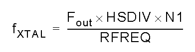
 As previously mentioned, the output frequency is the result of the DCO frequency divided by the product of two divisors. The DCO frequency is the product of a crystal frequency in the 114.25 MHz range and a settable reference frequency and must remain within the range of 4.85 to 5.67 Ghz. RFREQ has 38 bits of resolution allowing for a theoretical frequency setting resolution of 0.09 ppb at the test frequency of 114.285 MHz.
The HSDIV and N1 values have additional restrictions on them, specifically HSDIV can have the values 4, 5, 6, 7, 9 or 11. N1 can be 1 or any even number up to 128 inclusive (1, 2, 4, 6, ... 128).
Typically at startup you would determine the fxtal value specifically for your chip:
 By interrogating the chip, one can determine the values for HSDIV, N1 and RFREQ. By knowing the default startup frequency, the crystal frequency can be calculated. In my case, HSDIV = 11, N1 = 8 and RFREQ is 0x2B6109f08. Dividing this value by 2^28 gives me 0x2b as the integer portion or 43 decimal. To figure out the fractional part one would divide 0x6109f08 (the least significant 28 bits of RFREQ) by 2^28. Working in decimal instead of hex:
0x6109f08 = 101752584 / 2^28 = 0.3790579140
Adding this to the integer portion gives me a RFREQ value of 43.3790579140. Plugging this and the other knowns into the formula above gives me:
fxtal = (56320000 * 11 * 8) / 43.3790579140 = 114252365.964832 or 114.252365 Mhz
The datasheet states that the crystal frequency is only accurate to +/- 2000 ppm at 114.285 Mhz, or about +/- 0.22857 so my device is within the pretty horrible specification.
So, running this the other way, the output frequency is found as:
fout = (114252365 * 43.3790579140) / 11 * 8 = 56319999.524391 = 56.32 Mhz
A guy could envision a mechanism wherein you output a WWV frequency and tweak RFREQ until zero beat and then store the value for future reference, but the known frequency technique will get you very close.
If the DCO frequency is only moved +/- 3500 ppm, the oscillator output will be phase continuous. This should make implementing protocols such as WSPR, JT65 and the like much cleaner than my previous work using the Parallax Propeller. Also, in theory there is .42 Hz frequency resolution capable which would allow for much closer FSK tone shifts used in WSPR than the 1Hz resolution I had with the propeller.
It is unclear from the datasheet what is precisely meant by the +/- 3500 ppm figure. One interpretation is that once you have moved a total of 3500 ppm from whatever frequency you last set using the "large frequency change technique", you would have to recalculate the RFREQ and divisor values and set them back to the device. In my experience, most of the Arduino implementations I have reviewed have taken a flavor of this approach. While this is certainly safe, it is unlikely to be necessary. The other interpretation I have of the datasheet is that you could move the DCO over its entire range without recalculating parameters and do it in a phase continuous manner as long as no single frequency change is more than 3500 ppm. My interpretation is that once you have changed the frequency by either of these mechanisms, the new DCO frequency (not the output frequency) becomes the new "center frequency" described in the datasheet. So, under my theory, you could move the output frequency a total of 5.67 - 4.85 GHz = 0.82 Ghz 3500 ppm at a time. Of course, this would require a different part than I have which only has a range of 10-160 Mhz. Under this theory, as long as you didn't jump more than 17.5 Mhz between frequency settings, you only have to recalculate RFREQ and the change in frequency could be done phase continuous. This theory I have not yet tested.
More to come...
The HSDIV and N1 values have additional restrictions on them, specifically HSDIV can have the values 4, 5, 6, 7, 9 or 11. N1 can be 1 or any even number up to 128 inclusive (1, 2, 4, 6, ... 128).
Typically at startup you would determine the fxtal value specifically for your chip:
0x6109f08 = 101752584 / 2^28 = 0.3790579140
Adding this to the integer portion gives me a RFREQ value of 43.3790579140. Plugging this and the other knowns into the formula above gives me:
fxtal = (56320000 * 11 * 8) / 43.3790579140 = 114252365.964832 or 114.252365 Mhz
The datasheet states that the crystal frequency is only accurate to +/- 2000 ppm at 114.285 Mhz, or about +/- 0.22857 so my device is within the pretty horrible specification.
So, running this the other way, the output frequency is found as:
fout = (114252365 * 43.3790579140) / 11 * 8 = 56319999.524391 = 56.32 Mhz
A guy could envision a mechanism wherein you output a WWV frequency and tweak RFREQ until zero beat and then store the value for future reference, but the known frequency technique will get you very close.
If the DCO frequency is only moved +/- 3500 ppm, the oscillator output will be phase continuous. This should make implementing protocols such as WSPR, JT65 and the like much cleaner than my previous work using the Parallax Propeller. Also, in theory there is .42 Hz frequency resolution capable which would allow for much closer FSK tone shifts used in WSPR than the 1Hz resolution I had with the propeller.
It is unclear from the datasheet what is precisely meant by the +/- 3500 ppm figure. One interpretation is that once you have moved a total of 3500 ppm from whatever frequency you last set using the "large frequency change technique", you would have to recalculate the RFREQ and divisor values and set them back to the device. In my experience, most of the Arduino implementations I have reviewed have taken a flavor of this approach. While this is certainly safe, it is unlikely to be necessary. The other interpretation I have of the datasheet is that you could move the DCO over its entire range without recalculating parameters and do it in a phase continuous manner as long as no single frequency change is more than 3500 ppm. My interpretation is that once you have changed the frequency by either of these mechanisms, the new DCO frequency (not the output frequency) becomes the new "center frequency" described in the datasheet. So, under my theory, you could move the output frequency a total of 5.67 - 4.85 GHz = 0.82 Ghz 3500 ppm at a time. Of course, this would require a different part than I have which only has a range of 10-160 Mhz. Under this theory, as long as you didn't jump more than 17.5 Mhz between frequency settings, you only have to recalculate RFREQ and the change in frequency could be done phase continuous. This theory I have not yet tested.
More to come...
Subscribe to:
Posts (Atom)