The Arduino Due Timers or Counter Timer (TC) as they are called are a bit different implementation from the 8 bit Arduino devices. There is a lot of functionality in the Due Timer Counter module and it is not a simple thing to describe it fully so I will likely break this into several postings.
The SAM3X8E CPU has 3 Timer Counters (TCs) named TC0, TC1, TC2. Each TC includes three identical 32-bit channels. Each channel can be independently programmed to perform a wide range of functions including frequency measurement, event counting, interval measurement, pulse generation, delay timing and pulse width modulation (PWM).
Each channel has three external clock inputs, five internal clock inputs and two multi-purpose input/output signals which can be configured by the user. Each channel drives an internal interrupt signal which can be programmed to generate processor interrupts.
The TC embeds quadrature decoder logic connected in front of the 3 timers and driven by TIOA0, TIOB0 and TIOA1 inputs. When enabled, the quadrature decoder performs input line filtering and decoding of quadrature signals. We will not be covering this feature in these postings.
The TC block has two global registers which act upon all three TC channels. The Block Control Register allows the three channels to be started simultaneously with the same instruction. The Block Mode Register defines the external clock inputs for each channel, allowing them to be chained.
Clocks are assigned to Timer Counters as follows:
- TIMER_CLOCK1 - MCK/2
- TIMER_CLOCK2 - MCK/8
- TIMER_CLOCK3 - MCK/32
- TIMER_CLOCK4 - MCK/128
- TIMER_CLOCK5 - SLCK
MCK is the master clock (84 MHz) and SLCK is the slow clock (32 kHz). It should be noted that it is possible to select the slow clock as the master clock, which case TIMER_CLOCK5 input is equivalent to the master clock. As will be seen later, TCs can be chained together using the TIOA0, TIOA1, TIOA2 as an external clock input for subsequent TCs allowing further division of the clock frequency. I may get into clock chaining in further detail in a separate post.
This rather daunting image is the Timer Counter block diagramme. It is not as bad as it looks.

Channel signals seen above are as follows:
- XC0, XC1, XC2 - External Clock Inputs
- TIOA - Capture Mode: TC Input, Waveform Mode: TC Output
- TIOB - Capture Mode: TC Input, Waveform Mode: TC I/O
- INT - Interrupt Signal Output
- SYNC - Synchronization Input Signal
Each channel is organized around a separate 32-bit counter. The value of the counter is incremented at each positive edge of the selected clock. When the counter has reached the value 0xFFFFFFFF and wraps around to 0x00000000, an overflow occurs and the COVFS bit in TC_SR (Status Register) is set. The current value of the counter is accessible anytime by reading the Counter Value Register, TC_CV. The counter can also be reset by a trigger. In this case, the counter value resets to 0x00000000 on the next valid edge of the selected clock following the trigger event.
At the block level, input clock signals of each channel can either be connected to the external inputs TCLK0, TCLK1 or TCLK2, or be connected to the internal I/O signals TIOA0, TIOA1 or TIOA2 for chaining by programming the TC_BMR (Block Mode) register.
Each channel can independently select an internal or external clock source for its counter via the TCCLKS bits in the TC Channel Mode register (TC_CMR).
- Internal clock signals: TIMER_CLOCK1, TIMER_CLOCK2, TIMER_CLOCK3, TIMER_CLOCK4, TIMER_CLOCK5
- External clock signals: XC0, XC1 or XC2
The selected clock can be inverted using the CLKI bit in TC_CMR. This allows counting on the opposite edges of the clock. There is a burst function which allows the clock to be validated when an external signal is high. The BURST parameter in the Mode Register defines this signal (none, XC0, XC1, XC2).
Note that in all cases, if an external clock is used, the duration of each of its levels must be longer than the master clock period and the external clock frequency must be at least 2.5 times lower than the master clock.
Here is a block diagramme of the clock selection logic:

We still have not covered clock control, operating modes, or triggers, but we will touch on these topics as we work through examples.
Ok, enough background about Due timers for now and on to the first practical example. In this example we will define a function that allows the configuration of a TC to generate a square wave at a relatively low frequency of the caller's choice.
Firstly, let's think about clocking our timer. We have a system clock speed of 84 Mhz that can be divided by 4 different divisors (2, 8, 32 and 128) and the slow clock. So, the available timer clock speeds are:
- 42 MHz
- 10.5 MHz
- 2.652 MHz
- 656.25 kHz
- 32 kHz
To start up a timer, we need to deal with at least 4 different bits of information when doing simple operations with TCs.
- The Timer Counter (TC) you wish to use
- The channel in that TC you with to use
- The IRQ if interrupts are used
- The frequency of the timer
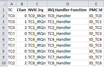
So, we will create a function to encapsulate all this to get a simple timer running. The timer will generate a square wave at the specified frequency.
There is a bit of housekeeping that needs to occur.
- We need to enable the ability to modify the power management controller's registers.
- We need to enable a specific peripheral clock specified by the IRQ.
- We need to set the TC configuration.
Power Management Controller calls look like this. We need to turn off write protection and then enable the peripheral clock for TC1 Channel 0.
pmc_set_writeprotect(false);
pmc_enable_periph_clk(ID_TC3);
You could also use TC3_IRQn rather than ID_TC3 as they are both different names for the same constant value. It is more clear to use the correct constant name, but as we will see shortly, it does simplify the implementation if we don't.
TC_Configure is used to configure a TC to operate in a given mode. The timer is stopped after configuration and must be restarted with TC_Start(). All interrupts of the timer are also disabled.
We will select Waveform Mode and instruct the TC to count up with a reset on register C (RC) compare. The following graphic depicts this mode, though it seems to imply the maximum counter value is 0xffff which is not true. With 32 bits, the maximum counter value would be 0xffffffff.
pmc_set_writeprotect(false);
pmc_enable_periph_clk(ID_TC3);
You could also use TC3_IRQn rather than ID_TC3 as they are both different names for the same constant value. It is more clear to use the correct constant name, but as we will see shortly, it does simplify the implementation if we don't.
TC_Configure is used to configure a TC to operate in a given mode. The timer is stopped after configuration and must be restarted with TC_Start(). All interrupts of the timer are also disabled.
We will select Waveform Mode and instruct the TC to count up with a reset on register C (RC) compare. The following graphic depicts this mode, though it seems to imply the maximum counter value is 0xffff which is not true. With 32 bits, the maximum counter value would be 0xffffffff.

TC configuration is accomplished with the following code. We will use Timer Clock 4 (master clock / 128 = 656.25 kHz) as for this example we will be generating low frequency waveforms. The function takes the TC and Channel as the first two parameters. The last parameter sets bits to indicate the fact we are in Waveform mode, only counting up to the maximum value specified in Register C (RC) and which of the 5 clocks we will use.
TC_Configure(tc, channel, TC_CMR_WAVE | TC_CMR_WAVSEL_UP_RC |
TC_CMR_TCCLKS_TIMER_CLOCK4);
Now we need to set Register A (RA) to be the clock count where our output (TIOA) goes high and Register C (RC) at the clock count where our output goes low. See the graphic above. We chose points that would generate a symmetrical 50% duty cycle square wave. Register C is set to the maximum count specified by the clock frequency divided by the desired frequency.
uint32_t rc = VARIANT_MCK / 128 / freq;
TC_SetRA(tc, channel, rc / 2); // 50% duty cycle
TC_SetRC(tc, channel, rc);
Now we enable the Register C (RC) compare interrupt. This bit is a little strange, because we have both an interrupt enable register and an interrupt disable register. I suspect this is so that a complete set of interrupts that you might need can be set in the interrupt enable list and sub-sets turned off by modifying the list of disabled interrupts. This way you don't have to remember which ones were enabled previously. This code enables only the RC compare interrupt and disables everything except RC compare interrupt, or so I believe.
tc->TC_CHANNEL[channel].TC_IER = TC_IER_CPCS;
tc->TC_CHANNEL[channel].TC_IDR = ~TC_IER_CPCS;
Start the timer running again.
TC_Start(tc, channel);
And tell the Nested Interrupt Controller to enable our IRQ.
NVIC_EnableIRQ(irq);
Simple, eh? Yeah... Nothing to it... Here is the entire function:
void TimerStart(Tc *tc, uint32_t channel, IRQn_Type irq, uint32_t freq)
{
pmc_set_writeprotect(false);
pmc_enable_periph_clk((uint32_t) irq);
TC_Configure(tc, channel, TC_CMR_WAVE | TC_CMR_WAVSEL_UP_RC |
TC_CMR_TCCLKS_TIMER_CLOCK4);
uint32_t rc = VARIANT_MCK / 128 / freq;
TC_SetRA(tc, channel, rc/2); // 50% duty cycle square wave
TC_SetRC(tc, channel, rc);
TC_Start(tc, channel);
tc->TC_CHANNEL[channel].TC_IER=TC_IER_CPCS;
tc->TC_CHANNEL[channel].TC_IDR=~TC_IER_CPCS;
NVIC_EnableIRQ(irq);
}
Whew... Still with me? Ok!
Now we will implement an ISR handler that just toggles the LED on digital pin 13 on and off every time the timer fires an interrupt. It also has to read the status of the Timer Counter (TC) in order to allow the next interrupt.
volatile boolean ledOn;
void TC3_Handler()
{
TC_GetStatus(TC1, 0);
digitalWrite(13, ledOn = !ledOn);
}
Ok, so given that we are only interrupting when Register C compare match occurs (see graphic above), and we are toggling pin 13 on every interrupt, we effectively divide the frequency that the led blinks at by two. If we want the frequency of the led blinking to match the frequency of the timer, we will need to interrupt on Register A compare match as well. The code changes to implement this would be to just enable the interrupt on RA compare as well as RC compare.
tc->TC_CHANNEL[channel].TC_IER= TC_IER_CPCS | TC_IER_CPAS;
tc->TC_CHANNEL[channel].TC_IDR=~(TC_IER_CPCS | TC_IER_CPAS);
So, the only thing remaining is to implement the setup function and stand back... We set the LED pin to output and initialize timer TC1, channel 0 using the IRQ TC3_IRQn (from the table above) with a frequency of 1 Hz.
void setup()
{
pinMode(13, OUTPUT);
TimerStart(TC1, 0, TC3_IRQn, 1);
}
So all of this is to blink a freaking LED at a 1 Hz rate. Amazing flexibility (and the associated complexity) comes at the bit of a steep learning curve. Here is the complete listing for your reference.
volatile boolean ledOn;
//TC1 ch 0
void TC3_Handler()
{
TC_GetStatus(TC1, 0);
digitalWrite(13, ledOn = !ledOn);
}
void TimerStart(Tc *tc, uint32_t channel, IRQn_Type irq, uint32_t freq)
{
pmc_set_writeprotect(false);
pmc_enable_periph_clk(irq);
TC_Configure(tc, channel, TC_CMR_WAVE | TC_CMR_WAVSEL_UP_RC |
TC_CMR_TCCLKS_TIMER_CLOCK4);
uint32_t rc = VARIANT_MCK / 128 / freq;
TC_SetRA(tc, channel, rc >> 1); // 50% duty cycle square wave
TC_SetRC(tc, channel, rc);
TC_Start(tc, channel);
tc->TC_CHANNEL[channel].TC_IER= TC_IER_CPCS | TC_IER_CPAS;
tc->TC_CHANNEL[channel].TC_IDR=~(TC_IER_CPCS | TC_IER_CPAS);
NVIC_EnableIRQ(irq);
}
void setup()
{
pinMode(13, OUTPUT);
TimerStart(TC1, 0, TC3_IRQn, 1);
}
void loop()
{
}
More to come, but have fun with this if you are so inclined. I am always willing to help out if you have questions. Drop me a note at ko7m at arrl dot net or comment here and I will do my best.
